Context
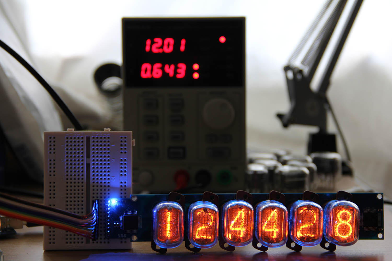
For those of you who don't already know, recently we ran a Kickstarter for our Nixie Tube Driver (NTD). The project was a huge success. To follow on from that, we ordered a second batch of drivers to put on our tindie store. The difference this time, however, is that we weren't building these drivers ourselves. For the first time, we decided to get our product manufactured in a PCB assembly house (if you're curious as to why: it turns out that making 100 drivers by hand in your bedroom is no fun at all...). As a result of this, we will be selling the drivers as a kit: all the SMD soldering is done, and the through-hole components are provided to solder yourself.
This presents a new challenge, how do we test the drivers when we recieve them from the assembly house?
PCB Test Methods
All PCBs need testing before they are deemed ready for use, but the methods of testing can range from simply an optical inspection (which is usually offered by default at most PCB assembly houses) to something much more involved, like paying a test engineer to run through a formalised procedure. Obviously with increased complexity comes increased cost, and how much you pay comes down to how critical the testing needs to be, and how complex.
Automated Self-Test
If your PCB involves some form of processing, then building in an automated self-test procedure is a no-brainer. Whenever I'm using a micro-controller in any project I try to include some form of this test. The principle of the test is fairly simple: you give your processor some way of introducing signals onto the board and measure how the board responds. If it responds as expected, brilliant! If not, then you can light an LED or spit something down the UART or let the user know in some way that something isn't right. This is useful in several ways: for one it gives you an idea of whether your board is working properly right when you turn it on, and for another if your board needs any calibration the self-test can become a self-cal very quickly.
It's also really easy to implement! It's a rare occurance for me to max out the capabilities of a micro-controller (I like having head room), so usually there's a spare DAC or SPI line somewhere around I can use to introduce signals onto my board, the extra cost of components to get the self-test in there is usually nothing compared to what it would cost to formally test every board. It also means if something goes wrong in the field, I've got code built in to diagnose it.
Bed of Nails Testing
If your board doesn't have any processing on it, or involves a significant amount of analog circuitry, the bed of nails test is probably worth thinking about. The idea is to marry pads on your board with a pre-built test circuit by pressing it down onto pins sticking up out of the test board (see image below). The pins can probe reference signals, clocks, or any important line on your board, and also introduce signals and measure them further down the signal chain. This can be particularly useful if you have circuitry like analog filters in a critical signal path, as these require large amounts of processing to test properly (Fourier Transforms and generating waveforms might well be out of the scope of your processor).
It's also usually very quick. While test procedures can run up to hours, the majority of them will usually take a couple of seconds, and being able to simply press the board to a fixture and hold it till it's finished is about as efficient as you get. Most importantly, it's a non-invasive procedure which works for surface mount components as well as through hole, making it ideal for basically any board you can think of (though I don't know if it would work for flat flex).
The problem with bed of nails testing, however, is that a professional service is expensive. And for simple boards it can be a little excessive.
The Nixie Tube Driver
The NTD presents a challenge. It has no micro-controller on it, rendering an automated self-test impossible, but a professional bed of nails test would be prohibitively expensive. Not testing the NTD was ruled out quickly as an option, as we were not as yet sure what quality the manufacturers would come back to us with. So how to test it? It is of course possible to test the NTD to some degree with a simple multimeter, testing the continuity of every line. Indeed, while making the kickstarter batch this needed doing several times. But with 100 boards and a test like this taking a good 10 minutes each, 16.7 hours of my time could be much better spent.
So why not spend that time making my own bed of nails test jig? Knowing the theory of operation of the boards well, and understanding the interface to them and the requirements for a test, this should be easy! Right?
Test Requirements
To successfully build an automated jig for the NTD, it is first beneficial to study the requirements of any such device. The test jig needs to be a bed-of-nails platform on which a single NTD (with only surface mount components soldered) can be placed, which will automate the process of testing the functionality of every digit of every segment of the NTD. It should also be able to check that there is a valid HV connection to every segment, and that the RGB backlights are functioning as they should.
To make the test useful any errors encountered in the test should be reported back to the us via a serial terminal, rather than simply stating whether the board has passed or failed. This reporting should be comprehensive, explaining in detail where an error was found, and what kind of error it was. This was specified to allow us to fix any broken boards, if they were fixable.
NTD Theory of Operation
So how do we go about doing this? Well to explain that it's first necessary to go through the operation of the NTD itself, as it will be impossible to design a test for an operation we don't understand.
The NTD is essentially a 65-bit open drain shift register. It consists of 2 HV5122 High Voltage shift registers in series, followed by a single D-type flip flop with its output to an open drain MOSFET configuration. When a number is displayed on the NTD it will flag the desired bit of the deisred segment, causuing the output of the shift register to pull LOW, in turn turning on the digit of the NTD. The schematic for the NTD can be found here.
The functional diagram of the HV5122 is shown to the right, showing how each pin activates the digit by pulling the line LOW.
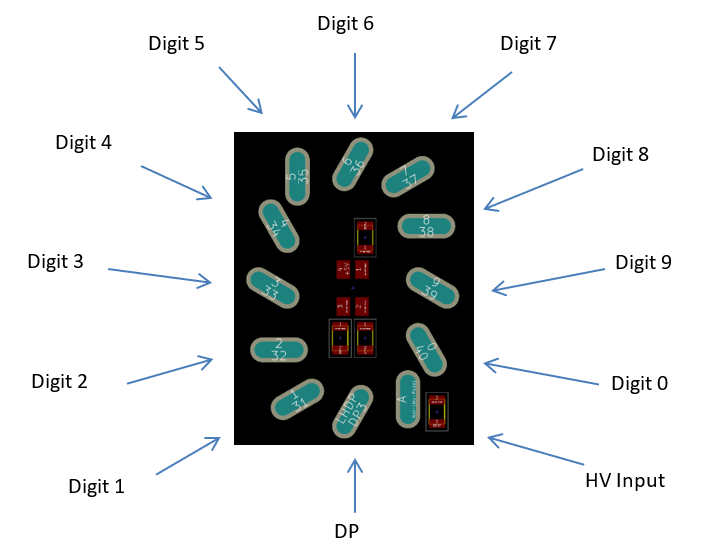
The segments and digits of the NTD are arranged in the manner shown above and to the left, and the shift register is arranged so the digits are triggered in order of 1-9 followed by 0 from segment 0-5, this is followed by the 5 available decimal points in order. This is explained in more detail in this document.
Combining this knowledge, the control bit stream is made up of 6 groups of 10 bit, corresponding to 1->9 followed by 0, followed by a group of 5 bits representing the decimal point. On receipt of a ‘1’, the open drain MOSFET will be turned ‘ON’ and the net will be pulled to GND. On receipt of a ‘0’ the net will be High-Z, and will float.
Theory of Test
Now we understand how the NTD works it is possible to design a test to make sure it is functioning correctly. The test principle in this case is simple: each net will be pulled to +5V with a 10K resistor, it will then be commanded to turn ‘ON’ and enable its open drain FET. This should pull the voltage to 0V and a micro-controller can sense this. While the net is low the micro-controller will test every other net to make sure there are no other net’s also turning ‘ON’. The high voltage lines will be tested by applying +5V at the socket, and testing whether we receive this at the header.
The main limit to this test method is that it requires being able to test every net, of which there are 65. This is undesirable, as it requires a high pin count microcontroller, and will be more complex to route on the board. To get around these issues it was thus decided to multiplex the test.
The groups for the multiplexing are split along segment, and along digit. This means that each segment will be powered individually, and each digit group (all the 7s or all the 8s etc.) can be tested at once. The digits not under test must be put in a high impedence (Hi-Z) state for this test to be effective, as if they weren't they would affect the segment under test.
Implementation
Now we know what we are testing, and how to test it, the test jig itself can be created.
Microcontroller
There is only really 1 obvious candidate for the microcontroller on the test jig: the ATMega328P. This is the micro used on the arduino, for which we have already written a software library to interface with the NTD with.
Segment Decoding
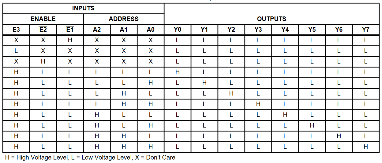
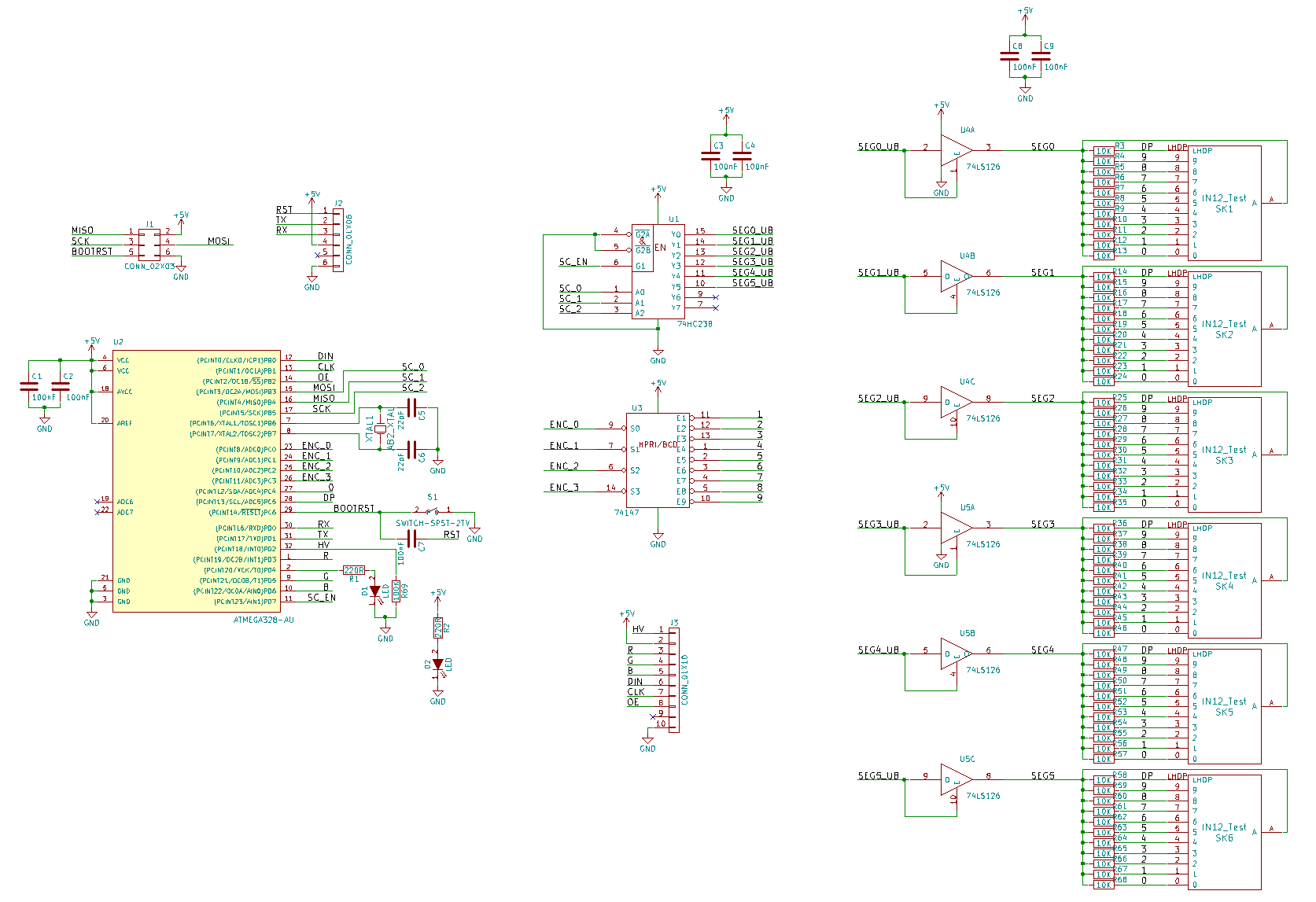
To facilitate the segment selection on the NTD test jig, a combination of a 74HC238 3-8 line decoder and 2 74HC126 tri-state buffer chips is used. The 3-8 line decoder is used to select which segment is active, and the tri-state buffers are used to put the segments not under test into the Hi-Z state required. When a segment is selected the microcontroller will address it via 3 lines to the decoder. These 3 lines will correspond to a binary number from 0-5, which will turn the output of the decoder HIGH for that segment. The truth table for the decoder is given below:
The #E1 and #E2 inputs to the decoder will be tied LOW, and the E3 input will be used as an output enable pin for the decoder.
The tri-state buffer function table is given to the right, each output of the decoder is fitted with one of these buffers. The 'OE' and 'A' pins on these buffers is tied together, ensuring the only 2 available states are either HIGH or Hi-Z, which is exactly what is required of the test jig.
By combining these 2 function tables together, the truth table below can be created for the segment selection. The final solution requires 4 outputs from the microcontroller, while allowing the selection of 6 seperate segments. This is a crucial saving, as the ATMega328P is not a microcontroller with a high pin count, thus any savings which can be made are beneficial.
Digit Encoding
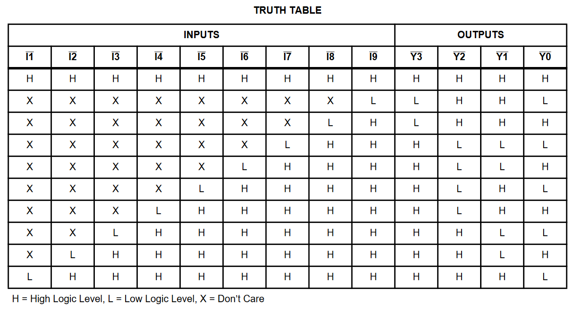
To read which digits of the NTD are 'ON' we must be able to read the state of all 11 digits on the NTD (0-9 and decimal point). The easiest way of doing this is to simply use 11 GPIO on the arduino, however, as we are trying to save as many pins as possible, a 74HC147 priority encoder will be used instead. The truth table for the encoder is given below:
The digits will be connected to their respective #I[X] pin, where X is the digit (i.e. digit 2 will be connected to #I2 etc). From this we will be able to see which is the highest numbered digit which is currently activated. Assuming that any short between digits of the NTD is bi-directional, this will be able to catch all shorts on the board. This is as if pin 9 and pin 4 are shorted together, when digit 4 is being tested, the encoder will return the result '9', showing which 2 pins are shorted. If there is an open circuit anywhere the encoder will return '15'.
Digit 0 and the decimal point will be tied directly to the ATMega to be tested individually. This is simply as there are not enough inputs to the decoder for them to also be routed via the decoder.
NTD Control
The NTD control lines must also be connected to the arduino, to allow the arduino to control the RGB backlight and the shift registers on the NTD. The pins for this were chosen according to the NTD wiring guide.
The final schematic for the test jig can be found below:
Test Sequence
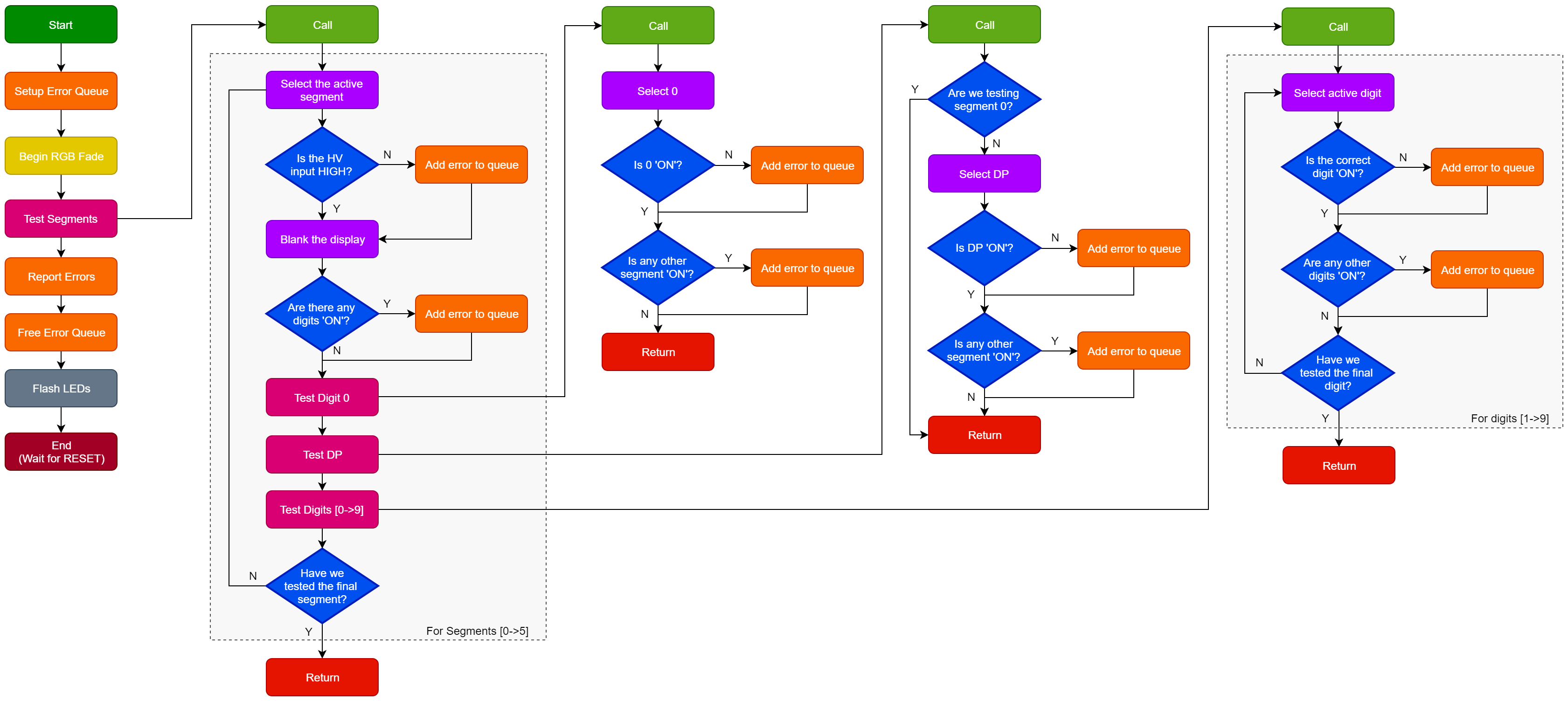
The sequence for the test of the NTD is summarised in the flowchart below. The test jig first sets up a queue in which it will store all errors encountered during the test. This queue can grow to accomodate the number of errors, and will be dynamically assigned as the test goes on. Then it begins the RGB fade, allowing us to assess whether the RGB LEDs are functioning. To perform the test a number of iterations are done, first through the segments (0-5) and then for each segments the digits are also iterated through (1-9). As the test progresses any errors found are added to the queue. Once the test is done, the queue is assessed and any errors are reported back over the UART, allowing us to make an assessment of what might be wrong. Finally the onboard LEDs are flashed to let us know the test is finished (though this also is printed to the UART). The test is designed to be run on each reset of the microcontroller, so the operator can place another NTD on the jig and then press the reset button and run the test.
The firmware running on the NTD test jig can be found on our github!
The Build
Now we'd established the theory, drawn up a schematic and established how the test sequence will be executed , the build could commence! This involved a PCB, some cool pogo pins, and soldering many many 10k resistors...
PCB
To bring the test jig to fruition, a PCB was created for the jig. This was designed around the NTD, using the same footprint for the pogo pins as is used for the nixie sockets on the NTD. The reset button was raised above the outline of the NTD to allow it to be pressed easily, and the header at the left hand end marries up with the header on the NTD.
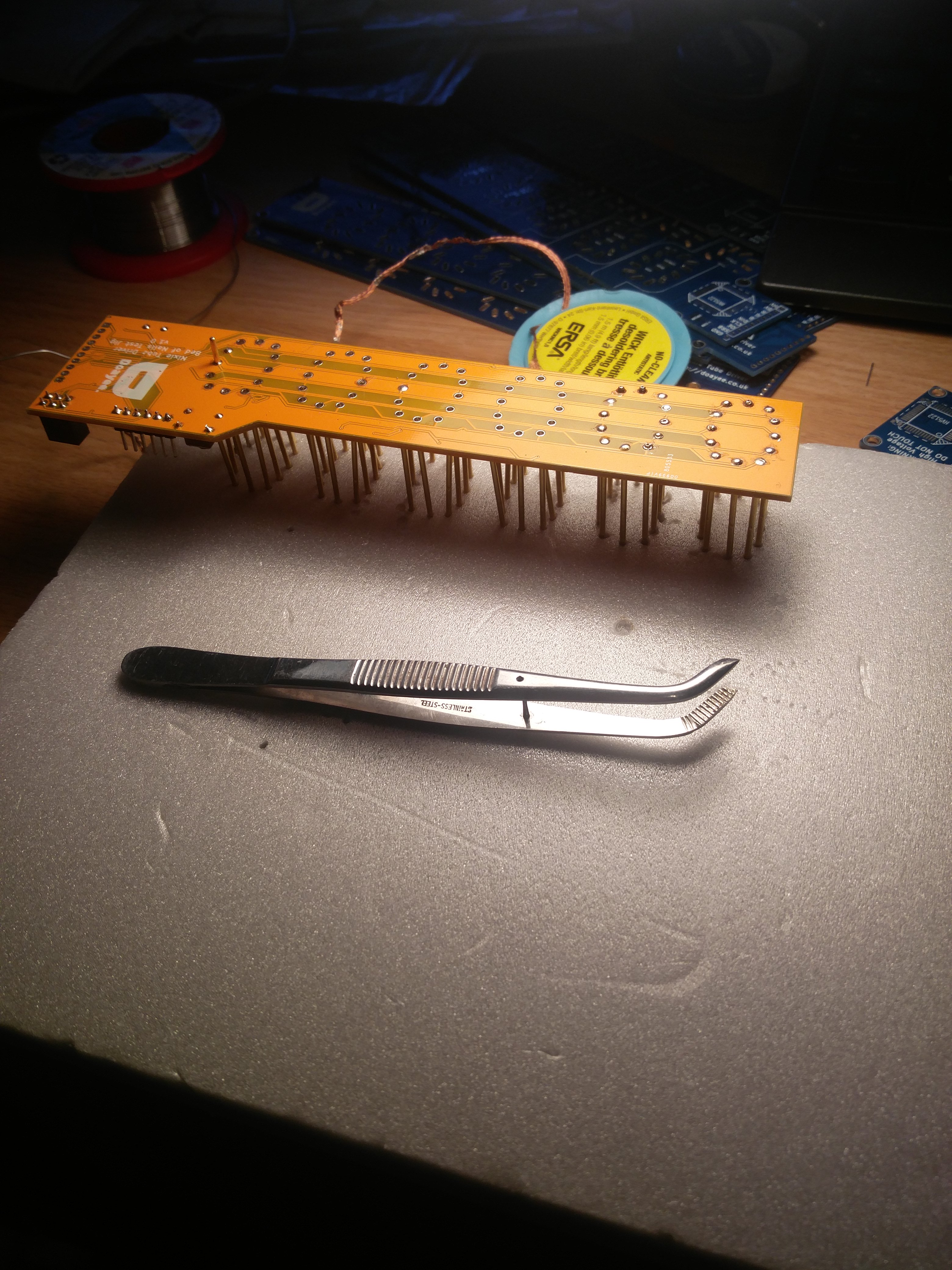
Once the PCB had arrived, it was time to solder it up. This was relatively straightforward, though soldering the pogo pins did prove to be tricky. To do this I first used the NTD as a stencil to punch holes in to a piece of packing foam. I then pushed the pogo pins into this foam 1 by 1 until then were all sticking out, then placed the test jig PCB on the back and soldered each one... It was a bit convoluted, but it got the job done!
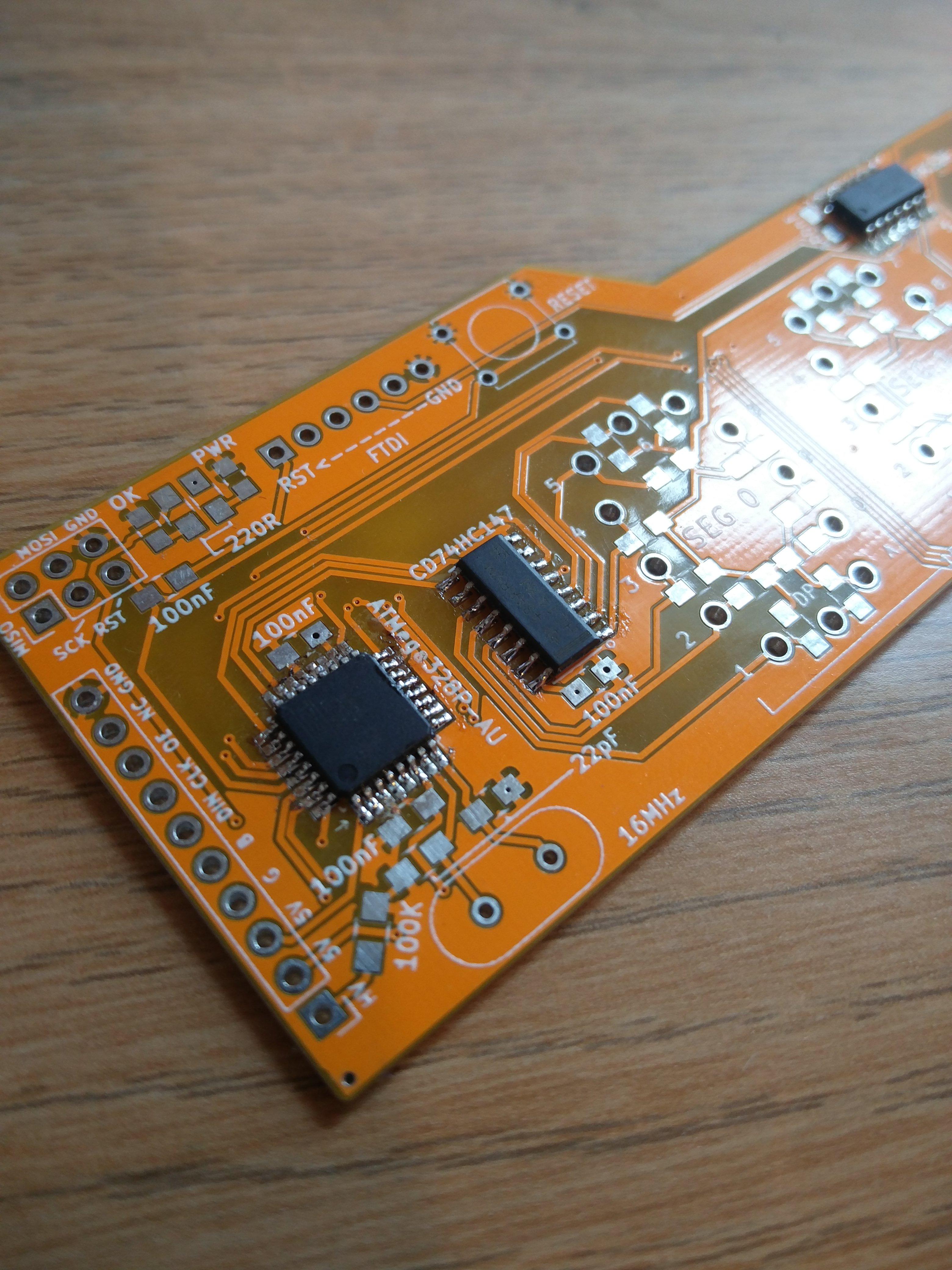
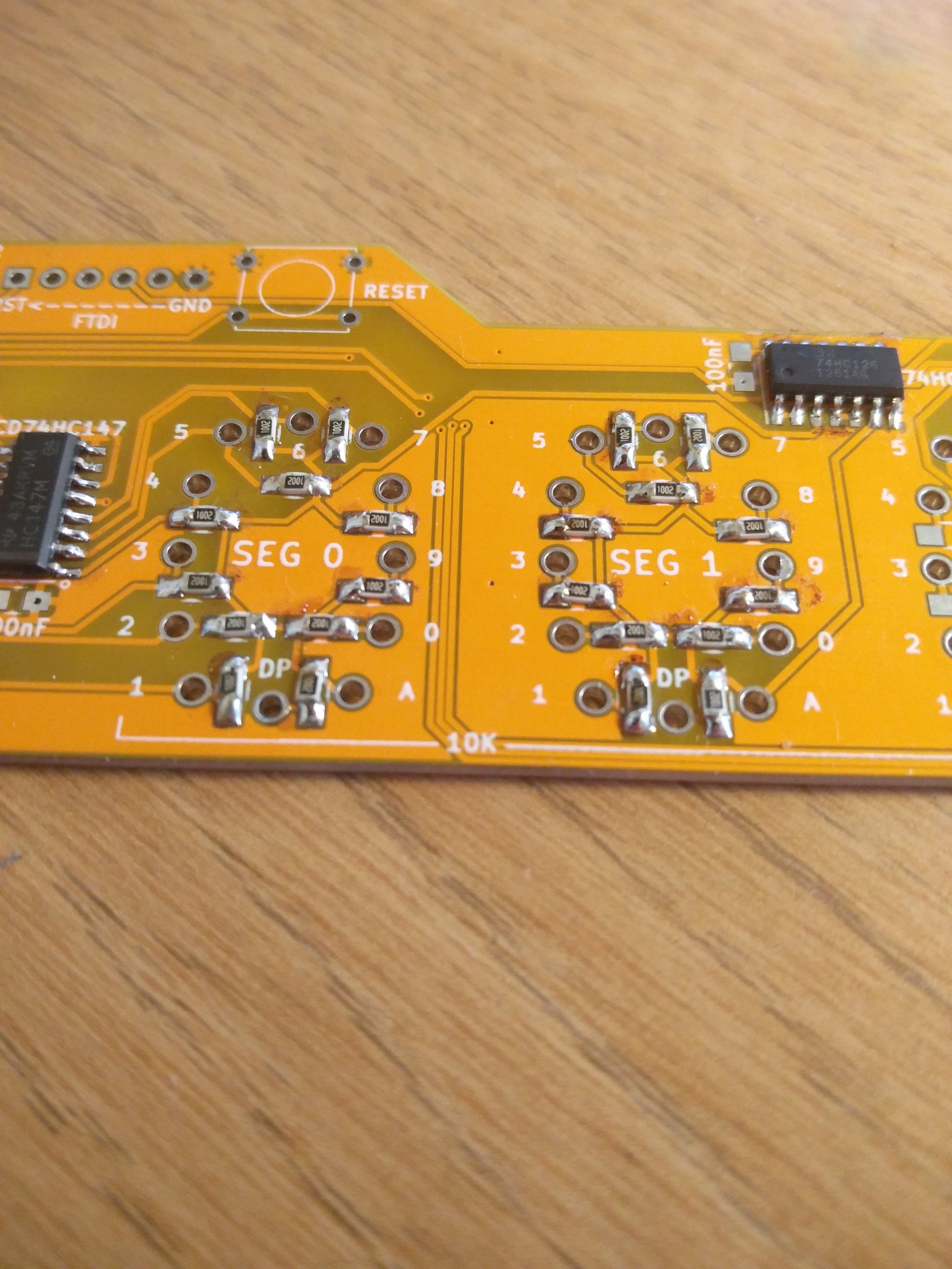
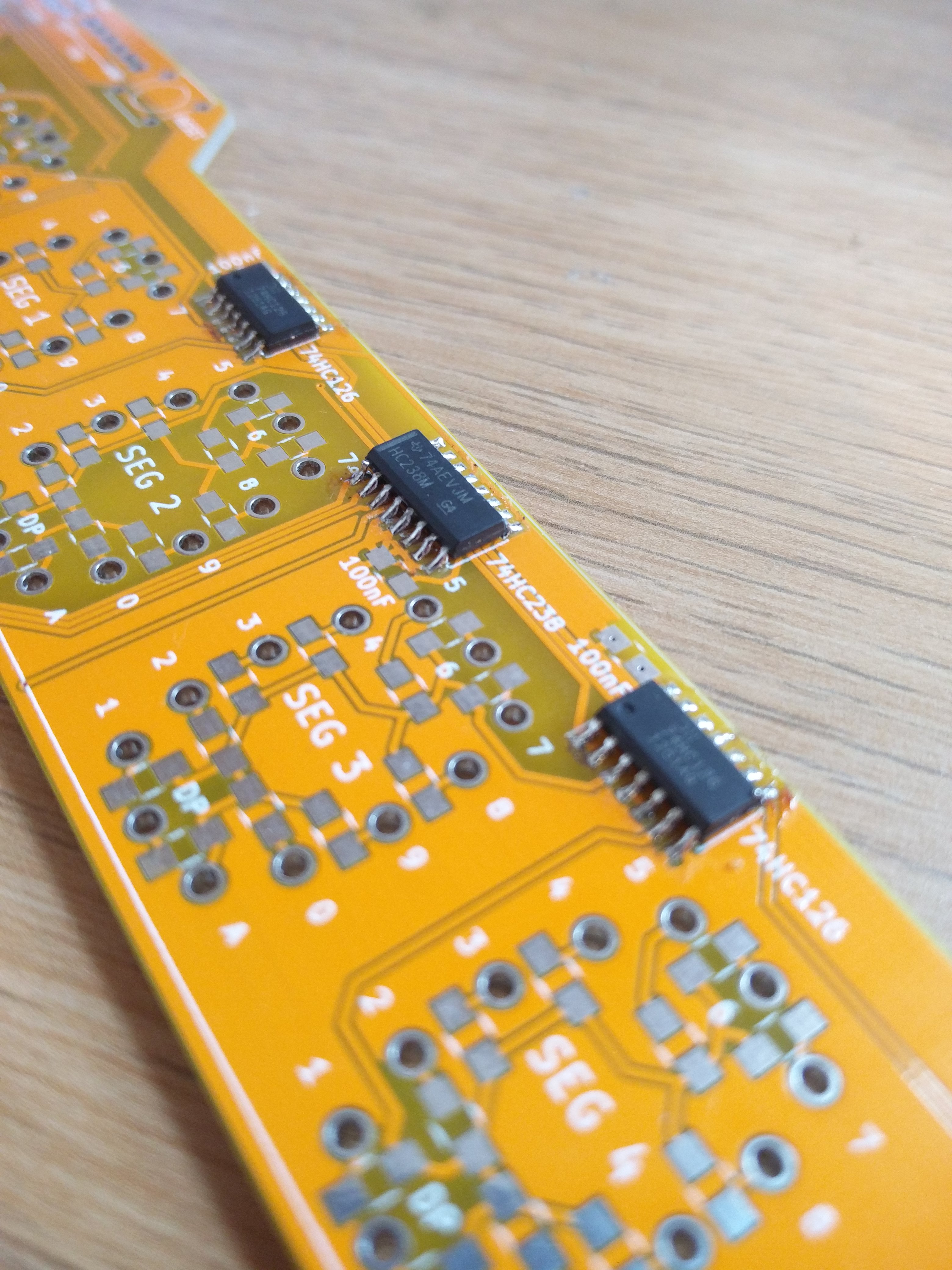
Photos of the build can be found below:
Conclusion
So the moment of truth... did it work?
Well I'm pleased to say yes! It worked a treat, and managed to slash the time it took to test each NTD from 10 minutes, to under 10 seconds. Overall it took about 10 hours of development (over the course of several months), including the build time, so that's a saving of about 6 hours in the end. Though if in future we need to do another run of NTDs, we'll have it ready.
And the final money shot: a box full of tested NTDs ready to be shipped to anywhere in the world... if you fancy one?









It’s useful to keep a ‘known-good’ board around, and at the beginning of testing, or when a suspect board is found, use it to verify that the test fixture is working properly.
Hi. Thanks for sharing. I just recently made my first bed-of-nails test jig design and found out that test failures due to bad pogo pin contacts onto cheap HASL PCBs were far more likely than actual errors in production. I even made a nice 3D-printed bed and clamp so that pogo pins were evenly pressed down, but the jig is still pretty useless for real-life testing because of false error rates. How reliable were the contact in your case? Did you have your test pads gold plated?
Thanks for your comment! The contacts in this case were fairly reliable, the pads they were mating up with were large through hole pads on the test PCB, so it was easy to apply a lot of presuure to them and have them reliably line up. The test pads were not gold plated, but we didn’t experience many issues.